

Understanding PCB assembly process is essential. PCB assembly is the process of soldering electronic components onto a bare printed circuit board to create a functional circuit. It follows a defined sequence, solder paste application, component placement, reflow or wave soldering, inspection, and testing, using one or more methods: surface mount technology (SMT), through-hole assembly, or a hybrid of both. The method chosen affects board density, mechanical strength, cost tier, and turnaround time.

What Is the PCB Assembly Process and How Does It Work?
PCB assembly transforms a bare, non-functional board into a working circuit by mounting and soldering electronic components onto it, the output is a PCBA ready for product integration.
This distinction matters for first-time buyers: PCB fabrication produces the bare board itself, the laminated substrate, copper traces, drilled holes, and surface finish. PCB assembly starts where fabrication ends, populating that board with resistors, capacitors, ICs, connectors, and every other component the design specifies. Ordering fabrication alone gets you a board you cannot use; assembly is what makes it functional.
Two documents drive every decision in the PCB assembly process. The bill of materials (BOM) lists every component by part number, value, and reference designator. The Gerber files define the board’s physical layout, copper layers, drill positions, and solder mask openings. Assemblers use both together to program pick-and-place machines, generate stencils, and verify placements before a single component is placed.
What Is the Difference Between SMT, Through-Hole, and Hybrid Assembly?
Three assembly categories cover the full range of board designs. Surface mount technology (SMT) places compact components directly onto pads on the board surface, it dominates modern, high-density designs. Through-hole assembly inserts component leads through drilled holes and solders them on the opposite side, offering stronger mechanical bonds for connectors and large passives. Hybrid assembly combines both methods on a single board, which is common when a design mixes fine-pitch ICs with heavy-duty connectors.
The finished PCBA is not simply a populated board, it is a tested, inspected assembly ready to drop into an enclosure, a product chassis, or a larger system. That distinction between “populated” and “integration-ready” is what separates a complete assembly run from a partial one.
Main Steps in the PCB Assembly Process
A standard PCB assembly process moves through solder paste printing, component placement, reflow soldering, inspection, and functional testing, in that fixed order.
What Is the Surface Mount Assembly Process and How Does It Differ from Other Methods?
Surface mount technology (SMT) dominates modern PCB assembly because it places components directly onto the board surface rather than threading leads through drilled holes, as through-hole assembly does. This allows far higher component density and supports automated, high-speed production lines.
The process opens with solder paste printing. A metal stencil, laser-cut to match the board’s pad layout, controls exactly how much paste deposits on each pad. Misalignment of even 0.1 mm at this stage causes bridging between adjacent pads or insufficient solder joints that only fail under thermal stress later. Catching stencil drift early is far cheaper than reworking a populated board.
Next, pick-and-place machines read component coordinates from a centroid file and position each part on its paste-covered pads. Placement accuracy directly determines reflow quality, a component shifted off-center can self-align during reflow or tombstone, standing upright on one pad instead of lying flat.
Reflow soldering then runs the board through a controlled thermal profile: preheat, soak, reflow peak, and cooling zones. Deviating from the profile, too fast a ramp, too high a peak temperature, or insufficient cooling, produces cold joints, component cracking, or delamination of the board substrate itself.
What Are Common PCB Assembly Defects and How Are They Detected?
Two inspection methods catch different defect classes. Automated optical inspection (AOI) uses cameras to flag surface-visible problems, missing components, polarity reversals, solder bridges, and tombstoning. It cannot see joints hidden beneath a package.
X-ray inspection fills that gap for ball grid arrays (BGAs) and other bottom-terminated components, where every solder joint sits under the package body. X-ray images reveal voids, cold joints, and bridging that AOI physically cannot reach.
After inspection, functional testing, including in-circuit testing (ICT) and board-level functional tests, applies power and signals to verify that the assembled board performs its intended electrical function. Skipping this gate does not eliminate defects; it moves discovery from the factory floor to the field, where repair costs and warranty claims multiply the original manufacturing cost many times over.
PCB Assembly Methods Compared: SMT, Through-Hole, and Hybrid
SMT suits high-density, high-volume builds; through-hole fits rugged, high-stress applications; and hybrid combines both where neither alone is sufficient.
Surface Mount Technology (SMT)
SMT dominates consumer electronics, smartphones, and compact IoT devices because surface-mount components occupy a fraction of the board area that leaded parts require. Smaller footprints allow designers to pack more circuitry onto both sides of the board, increasing density without increasing board size.
Automated pick-and-place machines handle component placement at speeds measured in thousands of parts per hour, which keeps labor content low. For volume production runs, this automation places SMT firmly in the budget-to-mid-range cost tier, the per-unit cost drops sharply as quantity rises.
Through-Hole Assembly
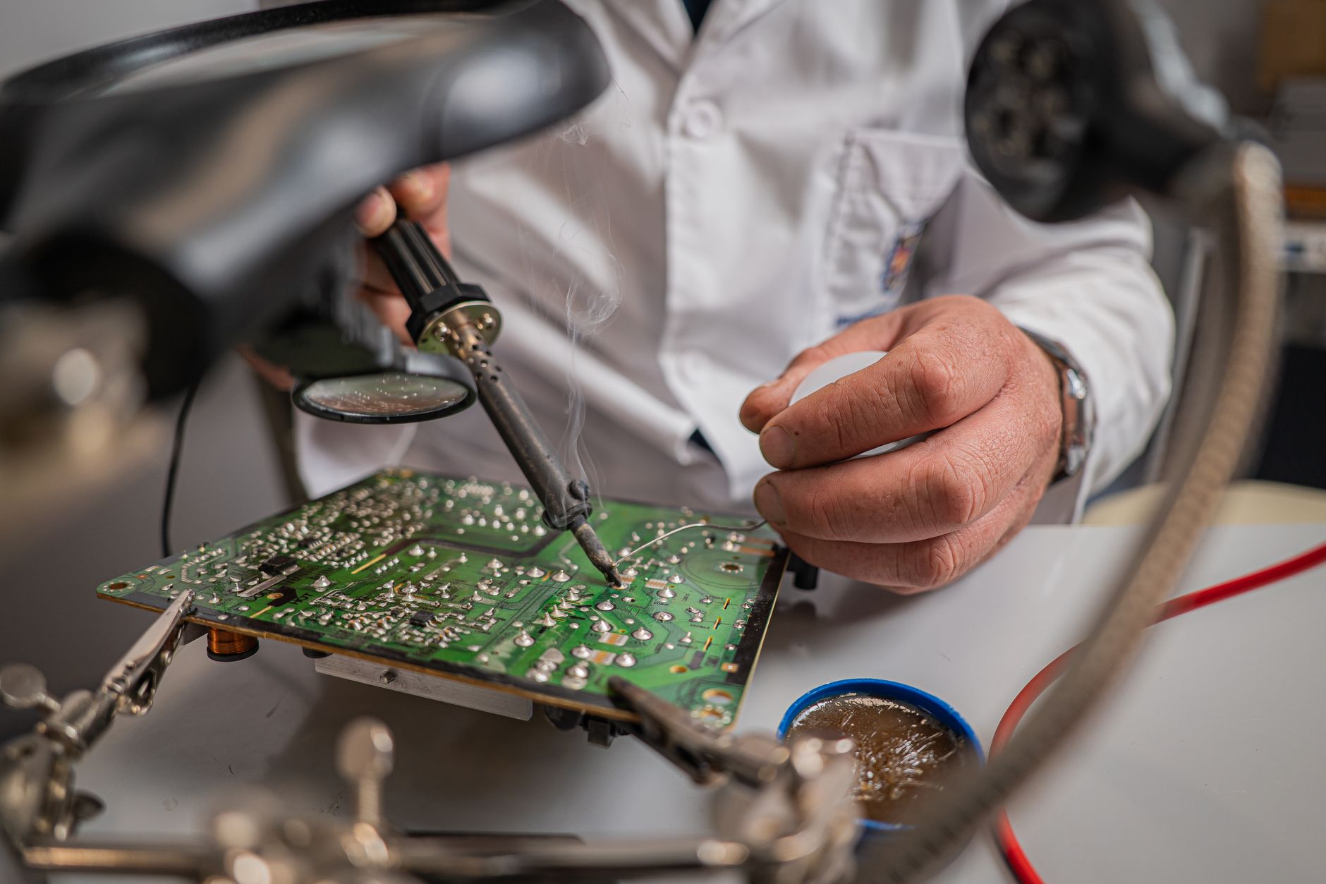
Through-hole components insert leads directly through drilled board holes, and the resulting solder joint bonds to the barrel of the hole rather than a surface pad. That mechanical connection withstands vibration, thermal cycling, and pull-out forces that surface-mounted pads cannot reliably handle, which is why connectors, large capacitors, and power components in aerospace, industrial, and military builds still use through-hole construction.
The trade-off is cost. Through-hole assembly requires manual insertion or specialized equipment, and wave-solder lines add process steps. For low-volume, high-reliability builds, through-hole sits in the premium cost tier.
Hybrid Assembly
Hybrid assembly runs SMT components, logic ICs, resistors, capacitors, alongside through-hole parts such as connectors and large electrolytic capacitors on the same board. This is the most common real-world PCB assembly process for industrial and medical equipment.
The sequencing challenge is significant: the board goes through reflow soldering for SMT components first, then through wave or selective soldering for through-hole parts. Each additional stage adds process time and handling risk.
How Do PCB Assembly Costs Compare Between SMT, Through-Hole, and Hybrid Methods?
SMT at volume is the most cost-efficient method because automation eliminates most manual labor. Through-hole commands a premium at any quantity due to insertion labor or selective-solder machine time. Hybrid sits between the two, it carries SMT’s automation benefit for the surface-mount portion but adds the cost of a second soldering stage for through-hole components.
What Are Typical PCB Assembly Turnaround Times and Lead Times?
SMT-only builds at volume move fastest because the entire process, paste printing, placement, and reflow, runs without manual intervention. Full automation allows some contract manufacturers to complete SMT runs in as little as one business day for simple boards at sufficient quantity.
Through-hole and hybrid builds extend lead time because wave soldering, selective soldering, or hand-soldering stages cannot be fully automated. Low-quantity hybrid orders in particular can take several additional days, since setup time for selective-solder fixtures becomes a significant share of total production time.
How Design and Quality Standards Shape PCB Assembly Outcomes
Design decisions made before a board reaches the line, and the compliance standards it must meet after, determine yield, rework rate, and whether the finished product can legally enter its target market.
What Are Design-for-Assembly (DFA) Best Practices and Guidelines?
Component spacing rules prevent pick-and-place collisions during placement. When components sit too close together, the placement head can clip an already-seated part, causing tombstoning or misalignment that only surfaces at inspection.
Pad geometry directly controls solder joint reliability. Pads that are too small starve the joint of solder; pads that are too large encourage bridging. Either condition produces a defect that IPC-A-610 inspection will flag, and that requires rework or board scrap.
Fiducial markers let AOI cameras and pick-and-place machines self-locate on the panel. Without correctly placed fiducials, machine vision loses its reference point, and placement accuracy degrades across the entire board.
When DFA problems surface at assembly rather than at design review, the costs compound quickly. A mismatched pad requires stencil rework, a new aperture cut or a full stencil replacement. A discontinued or non-footprint-compatible component triggers substitution searches. A fundamental layout error forces a board re-spin, which adds weeks and tooling cost to the PCB assembly process.
What PCB Assembly Compliance Standards Matter: RoHS, REACH, and IPC?
IPC-A-610 defines acceptability criteria for solder joints, and IPC-2221 governs generic design rules, together they form the shared language between designer and assembler. Specifying a class matters: Class 1 covers general electronics with minimal inspection rigor, Class 2 applies to most industrial and consumer products, and Class 3 governs life-critical or aerospace assemblies where every joint must meet the tightest acceptance criteria. Moving up a class raises the inspection threshold and directly affects yield expectations and cost tier.
RoHS (Restriction of Hazardous Substances) restricts lead, mercury, cadmium, and several other substances in solder and component materials. REACH governs chemical substances throughout the supply chain, including materials in laminates and surface finishes. Non-compliance with either directive blocks market access across the EU and in many jurisdictions that have adopted equivalent legislation, making both standards non-negotiable for any product destined for international distribution.
What to Look for When Choosing a PCB Assembly Manufacturer
The right PCB assembly manufacturer combines verified equipment, recognized certifications, and proactive communication, not just a competitive quote.
What Manufacturing Equipment and Capabilities Indicate Quality PCB Assembly Services?
Equipment tells you what a manufacturer can actually build. High-speed pick-and-place machines with fine-pitch capability, typically 0201 components or smaller, are a baseline requirement for modern SMT work. Closed-loop AOI after the reflow stage catches solder defects before they compound, and X-ray inspection is the only reliable method for verifying BGA joint integrity beneath the package. A facility without X-ray capability is a genuine risk on any board with hidden-joint components.
Certifications function as verifiable proxies for process discipline, not marketing badges. ISO 9001 governs the quality management system, documentation, corrective action, and traceability. IPC-A-610 trained operators follow a defined workmanship standard for solder joints and component placement. UL-recognized processes signal that the electrical safety requirements of the PCB assembly process have been independently evaluated. Ask for certificates with issue dates; expired or unrenewed credentials indicate a lapsed commitment.
Service model choice affects who carries procurement risk. Turnkey assembly, where the manufacturer sources all components, reduces your coordination burden but requires confidence in their supply chain. Consigned (kitted) assembly gives you direct control over component sourcing, but you absorb the logistics responsibility and any shortage delays.
The clearest differentiator between manufacturers is pre-production feedback. A supplier who flags BOM conflicts, missing part numbers, or pad geometry mismatches before the line runs saves days of rework. One who simply executes the job as submitted passes that risk back to you.

Frequently Asked Questions
What is the difference between PCB fabrication and PCB assembly?
PCB fabrication produces the bare board, the laminated substrate with etched copper traces, drilled holes, and applied solder mask. PCB assembly is the subsequent process of populating that bare board with electronic components. The two are distinct manufacturing stages: fabrication creates the physical foundation; assembly makes it functional. Many contract manufacturers offer both under one roof, which reduces handling time and simplifies quality control across the full production chain.
What files does a PCB assembler need to get started?
A PCB assembler typically requires a Gerber file set for the board layout, a Bill of Materials (BOM) listing every component with part numbers and quantities, and a pick-and-place (centroid) file that maps each component’s X/Y coordinates and rotation on the board. Some assemblers also request an IPC-2581 or ODB++ file as an alternative to Gerbers. Providing complete, accurate documentation up front prevents production delays caused by component substitutions or placement errors.
Can through-hole and SMT components be assembled on the same board?
Yes, mixed-technology assembly combines surface-mount and through-hole components on a single board, and it is common in designs that require both high-density SMT ICs and mechanically robust through-hole connectors or capacitors. The board typically goes through SMT placement and reflow first, then through-hole insertion and wave soldering or selective soldering afterward. Sequencing matters: the reflow oven must not damage any through-hole parts already placed, so assembly planning is critical.
What does IPC Class 2 versus Class 3 mean for PCB assembly quality?
IPC Class 2 covers general electronics products where extended service life is required but uninterrupted operation is not critical, consumer electronics and most commercial devices fall here. IPC Class 3 applies to high-reliability products where failure is not acceptable, such as aerospace, military, and medical equipment. Class 3 demands tighter solder joint acceptance criteria, more rigorous inspection, and stricter process controls throughout assembly. Specifying the correct class before production prevents costly rework or re-qualification later.
Conclusion
The PCB assembly process is a precise sequence where each stage, solder paste application, component placement, reflow, inspection, and testing, directly affects the reliability of the finished board. Two decisions have outsized impact on outcomes: choosing the right assembly method (SMT, through-hole, or mixed) for your design, and specifying your IPC quality class before production begins, not after.
If you are preparing a new design for assembly, audit your BOM and pick-and-place file against your chosen assembler’s component sourcing capabilities before you submit. Mismatches at that stage cause more delays than any step in the process itself.
Recommended Articles
Explore more from our content library:
- A Complete Guide to Understanding Turnkey Manufacturing
- <a href="https://gcnov.com/what-is-box-build-assembly-complete-guide-for-electronics/" title="Box Build Assembly Guide for Electronics Manufacturers“>Box Build Assembly Guide for Electronics Manufacturers
- <a href="https://gcnov.com/what-is-sheet-metal-bending-process-tolerances-industrial/" title="Complete Guide to Sheet Metal Bending Processes and Uses”>Complete Guide to Sheet Metal Bending Processes and Uses
- Core Processes and Applications of Sheet Metal Stamping
- <a href="https://gcnov.com/what-is-pcba-assembly-complete-process-guide-for/" title="Complete Guide to the PCBA Assembly Process for Electronics”>Complete Guide to the PCBA Assembly Process for Electronics
