

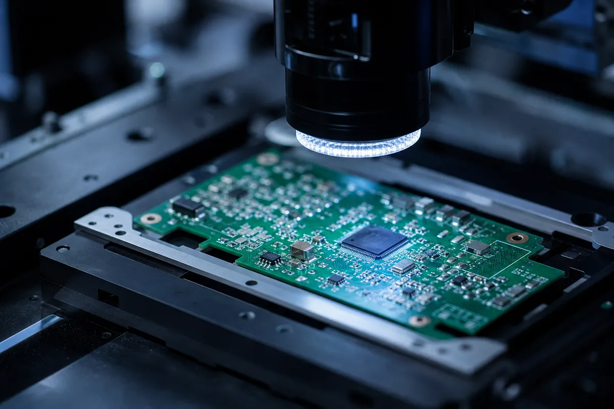
PCBA quality assurance is the set of testing, inspection, and validation procedures used throughout printed circuit board assembly to catch defects before boards reach customers. It combines automated checks (AOI, X-ray, ICT), manual visual inspection, and functional testing at incoming, in-process, and final stages, all measured against standards like IPC-A-600 and IPC-A-610. For manufacturers serving medical devices or industrial automation, it matters because a single undetected solder bridge or cold joint can cause field failures, recalls, or safety incidents downstream.
What Is PCBA Quality Assurance and Why Does It Matter for Manufacturers?
PCBA quality assurance is a structured discipline built into every stage of production, not a single inspection performed after boards come off the line.
What Does PCBA Stand For and What Role Does Quality Assurance Play in the Manufacturing Process?
PCBA stands for printed circuit board assembly, the finished product once components are soldered onto a bare board. Quality assurance in this context covers incoming material checks, in-process monitoring during solder paste application and reflow, and final electrical and functional testing. Treating QA as a sequence rather than a checkpoint matters because defects introduced early, like a misaligned stencil or a contaminated component reel, tend to surface as failures much later if nobody catches them in between. A manufacturer running PCBA quality assurance correctly checks the board at each handoff: after solder paste printing, after placement, after reflow, and again after final assembly.
What Industry Standards Like IPC-A-600 and IPC-A-610 Guide PCBA Quality Assurance?
Two IPC standards anchor most PCBA quality programs, and they cover different things. IPC-A-600 defines acceptability criteria for bare printed circuit boards, trace width, plating, hole quality, before any components go on. IPC-A-610 governs the assembled board: solder joint quality, component placement, cleaning, and marking. Manufacturers reference both because a defect can originate in the bare board or in the assembly process, and passing one standard says nothing about the other.
The cost logic behind this is straightforward. A defect caught at incoming inspection might cost a few cents in rework. The same defect discovered after a device ships can trigger a recall, a warranty claim, and lasting damage to a customer relationship. That escalation is why regulated sectors, medical devices, industrial automation, automotive, often require IPC Class 3 acceptance, the strictest tier, where consumer electronics typically ship at Class 2.
What Are the Main Testing Methods and Inspection Techniques Used in PCBA Quality Assurance?
Effective PCBA quality assurance combines seven distinct testing methods, each catching a defect class the others miss, applied at specific points along the production line.
What Are the Seven Primary PCB and PCBA Testing Methods, and When Should Each Be Used?
Automated optical inspection (AOI) uses cameras to scan solder joints, component placement, and polarity right after reflow, catching visible defects like tombstoning or missing parts before boards move forward. X-ray inspection (AXI) picks up where AOI’s cameras can’t see, checking hidden solder joints under ball grid arrays (BGAs) and other leadless packages where voids or bridging would otherwise go undetected.
In-circuit testing (ICT) uses bed-of-nails fixtures to verify individual component values, shorts, and opens at the electrical level, it isolates a bad resistor or capacitor before the board ever powers on as a system. Functional circuit testing (FCT) checks the opposite end of the problem: it powers the assembled board and confirms it behaves correctly under real operating conditions, catching firmware or system-level interaction faults that ICT can’t see.
Flying probe testing serves as a fixture-free alternative to ICT, useful for low-volume or prototype runs where building a dedicated test bed isn’t cost-justified. Manual visual inspection still has a role for mechanical details a machine may misjudge, like connector seating or mechanical damage. Burn-in and environmental stress testing expose boards to improved temperature, humidity, or vibration over time, surfacing latent defects that would otherwise fail early in the field.
What’s the Difference Between Incoming Inspection, In-Process Testing, and Final Quality Control?
Incoming inspection verifies raw PCBs and components before assembly even starts, confirming supplier material meets specification. In-process testing runs checks between assembly stages, AOI after paste printing, again after reflow, to stop defects before more labor gets added to a bad board. Final quality control applies ICT, FCT, and sometimes burn-in as a last checkpoint before shipment.
Production volume, board complexity, and end-use risk determine which mix makes financial sense. A high-volume consumer board might rely mainly on AOI and ICT, while a low-volume medical or industrial board, where field failure carries higher stakes, often justifies the added cost of X-ray and burn-in testing.
How Do AOI, Manual Inspection, and AI-Based Testing Compare for PCBA Defect Detection?
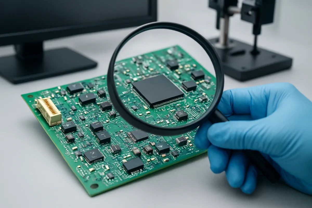
AOI catches placement and solder defects fast and consistently, manual inspection catches what rules miss, and AI-based systems learn from both to cut escape rates over time. Each method fits a different point in a PCBA quality assurance program, and most serious production lines use all three.
Where AOI Excels and Where It Misses
Automated optical inspection scans boards at high speed, flagging tombstoning, missing components, bridging, and insufficient solder against fixed thresholds. It’s repeatable, the same board gets the same verdict at 2 a.m. or 2 p.m., which matters when a line runs three shifts.
The blind spot is physical: AOI cameras can’t see solder joints hidden under a ball grid array or shielded component. Rule-based systems also throw false positives when lighting or board color varies slightly, forcing an operator to re-check parts that were actually fine.
What Manual Inspection Still Catches
Manual inspection remains the fallback for ambiguous cases, a solder joint that looks marginal but isn’t in any defect library, or a component substitution an operator recognizes but a camera doesn’t. Experienced inspectors catch novel failure modes AOI hasn’t been programmed to see.
The tradeoff is consistency. Fatigue and shift changes introduce variability that a machine doesn’t have, and manual inspection is slower per unit than automated scanning.
What Are the Cost-Benefit Tradeoffs Between Automated Optical Inspection, Manual Inspection, and Machine Learning-Based Defect Detection?
Manual inspection suits low-volume or prototype runs where programming an AOI system isn’t worth the setup time; AOI pays off at mid-to-high volume once defect libraries are built out; AI-enhanced inspection is a premium layer justified when escape rates at scale carry real cost, recalls, warranty claims, field failures in medical or industrial equipment.
How Are Emerging Technologies Like AI and Machine Learning Changing PCBA Quality Assurance in 2025?
Machine learning-based inspection systems learn defect patterns directly from image data instead of relying on fixed pixel thresholds, which lowers false-positive rates as the model sees more boards. That reduces the manual reprogramming cycles AOI traditionally requires with each new board revision. Going into 2025, these systems increasingly link inspection results to traceability data, tying a detected defect back to a specific reflow cycle, solder lot, or operator shift for faster root-cause analysis.
What Are the Most Common PCBA Defects and How Do You Identify Them?
The recurring defects in PCBA manufacturing fall into a handful of categories, solder bridges, cold joints, component misalignment, insufficient paste, lifted leads, and BGA voiding, each with a distinct visual or X-ray signature. Good PCBA quality assurance depends on inspectors and machines recognizing these signatures fast, before a board reaches functional test or a customer’s hands.
What Are the Typical PCBA Defects—Solder Bridges, Cold Joints, Component Misalignment—and How Do You Spot Them Visually?
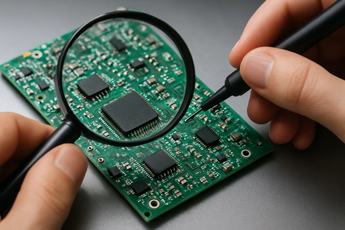
A solder bridge is an unintended connection between adjacent pads, usually caused by excess paste or a misprinted stencil. Under magnification it shows up as a shiny blob of solder spanning two pads that should be isolated, an easy catch for automated optical inspection (AOI) trained on that footprint.
Cold or dry joints happen when solder doesn’t reach full reflow temperature, leaving a mechanically weak connection. Visually, a good joint looks smooth and glossy; a cold joint looks grainy, dull, or cracked, sometimes with a visible gap between the lead and pad.
Component misalignment includes tombstoning, where one end of a small passive lifts off the pad during reflow, and general skew, where a part sits offset from its printed footprint. Both are visible as a clear mismatch between the component’s actual position and the silkscreen outline underneath it.
Other frequent issues include insufficient solder paste deposition, leads that lift away from the pad after cooling, and voiding inside BGA joints, hidden defects that only X-ray inspection can reveal, since the solder balls sit underneath the package.
What Can Manufacturers Learn From PCBA Failure Case Studies and Defect Analysis?
Finding a defect only solves half the problem, root-cause analysis is what stops it from repeating. If AOI flags a solder bridge pattern on one board, the real fix usually traces back to stencil aperture design, paste volume, or reflow profile settings, not just that one unit.
Structured defect logging turns individual failures into a pattern. Tracking defect type against production line, shift, operator, and component lot batch often surfaces a recurring failure mode, say, cold joints appearing only on second-shift runs, pointing to a reflow oven calibration drift rather than a one-off mistake.
How Do You Implement a PCBA Quality Assurance Program in Your Manufacturing Operation?
Build PCBA quality assurance in four phases, standards and training, incoming inspection, in-line AOI/ICT, and final QC with documentation, rather than trying to install everything at once.
Phase one is adopting a standard (IPC-A-610 is the common reference point for assembly acceptability) and training operators against it. Phase two adds incoming-inspection procedures so bad components never reach the line. Phase three layers in automated optical inspection and in-circuit testing at the points where defects are cheapest to catch. Phase four locks down final QC, functional test, packaging inspection, and traceability records tied to each lot. Skipping ahead to automation before staff can read a defect on sight tends to produce expensive tools operated on guesswork.
What’s a Realistic Timeline and Resource Plan for Small-to-Medium Manufacturers to Build a PCBA QA Program?
Start with people, not machines: train existing operators on visual inspection and defect classification before buying automated equipment.
A small manufacturer can run manual visual inspection and basic incoming checks with almost no capital outlay. As volume grows, phase in AOI on the highest-runner product lines first, then ICT once fixture costs are justified by unit count. Tie each equipment purchase to a volume or defect-rate trigger rather than a calendar date, that keeps spending aligned with actual risk instead of a generic rollout schedule.
How Do You Measure ROI and Set Quality Metrics for Your PCBA Quality Assurance Process?
Track defect rate in parts-per-million (DPPM), first-pass yield, and escape rate to the customer as your core quality KPIs.
DPPM shows how clean your process is at the board level; first-pass yield shows how much rework your line is absorbing before shipment; escape rate shows what customers actually experience. The ROI mechanism is straightforward even without a precise multiplier: every defect caught on the line costs less than the same defect caught in the field, where it triggers a return, a warranty claim, or a line-down call from a customer. Inspection equipment and training are the upfront cost; avoided rework, returns, and field failures are the payback.
Before rolling a new program across the whole plant, pilot it on one line or one product family. At My Website, we apply this phased approach across our own PCBA and turnkey EMS work, standards first, inspection layered in as volume justifies it, metrics tracked from the first build, so customers in regulated fields like medical devices and industrial automation get a documented, repeatable process rather than a one-off inspection pass.
Frequently Asked Questions
What is the difference between IPC-A-600 and IPC-A-610?
IPC-A-600 covers acceptability standards for bare, unpopulated printed circuit boards, while IPC-A-610 governs finished, assembled electronic assemblies. In practice, IPC-A-600 checks the board itself, plating, hole quality, laminate condition, before components go on. IPC-A-610 takes over after assembly, judging solder joints, component placement, and cleanliness against the acceptance class the buyer specifies.
Can small manufacturers implement PCBA quality assurance without expensive equipment?
Yes, small manufacturers can build a credible quality program before investing in high-end automated equipment. Starting with documented visual inspection against IPC-A-610 criteria, basic continuity checks, and disciplined incoming-material inspection covers much of the risk. AOI and flying probe testing add coverage as volume grows, but process discipline and traceability matter more early on than equipment cost.
How often should AOI programming be updated for a production line?
AOI programs need review at every engineering change order and any time a new component, footprint, or supplier is introduced. Even without design changes, periodic re-verification against known-good and known-bad boards catches drift in camera calibration or lighting that could let real defects pass or trigger nuisance false calls.
What acceptance class should medical device PCBAs meet?
Most medical device PCBAs are held to IPC-A-610 Class 3, the standard for high-reliability electronics where failure isn’t acceptable. Class 3 applies tighter solder joint, spacing, and cosmetic criteria than Class 2, reflecting the continued performance and traceability demands of implantable, diagnostic, and life-sustaining equipment.
Does 100% inspection eliminate the need for functional testing?
No, 100% visual or automated optical inspection does not replace functional testing. AOI and X-ray catch physical defects like solder bridges or misalignment, but only in-circuit testing and functional test verify that the assembled board actually performs its intended electrical function under real operating conditions.
Conclusion
Defect-free PCBAs come from layered verification, not a single inspection step. Combine incoming material checks, AOI or X-ray, ICT, and functional testing, and anchor acceptance criteria to IPC-A-610 class requirements matched to your product’s risk level, Class 3 for medical and industrial control boards, Class 2 for most commercial work. Document everything; traceability is what turns a quality claim into evidence when a customer or auditor asks for it.
Next step: pull your current inspection checklist and confirm it references a specific IPC-A-610 class by name, if it doesn’t, that’s the first gap to close.
Recommended Articles
Explore more from our content library:
- <a href="https://gcnov.com/what-is-rapid-prototyping-in-manufacturing-from-cad-to/" title="How Rapid Prototyping Manufacturing Turns CAD Into Parts”>How Rapid Prototyping Manufacturing Turns CAD Into Parts
- <a href="https://gcnov.com/what-is-design-for-manufacturability-dfm-engineering-best/" title="Design for Manufacturability Best Practices for Suppliers”>Design for Manufacturability Best Practices for Suppliers
- Precision Tolerance Manufacturing Explained With Examples
- What Is Turnkey Electronics Manufacturing for PCBA?
- The Process and Applications of Precision Metal Grinding
