

The PCBA assembly process is the sequence of steps that transforms a bare printed circuit board (PCB) into a fully functional Printed Circuit Board Assembly (PCBA) by mounting and soldering electronic components onto it. Unlike a PCB, which is just the blank board, a PCBA carries all the components needed to perform a circuit function. The process typically spans solder paste application, component placement, reflow or wave soldering, inspection, and testing, with the exact method depending on component types and product requirements.

What Is PCBA and How Does It Differ from PCB?
A PCB is the bare substrate, copper traces on laminate, no components, while a PCBA is the finished, functional board with every component soldered in place.
The distinction is more than semantic. A PCB is a material; a PCBA is a product. One sits in a warehouse awaiting assembly; the other powers a device. Confusing the two terms when placing orders creates real procurement problems: suppliers quote differently for each, lead times are calculated separately, and quality standards such as IPC-A-610 apply specifically to the assembled board, not the bare substrate.
Design decisions made before the PCBA assembly process begins also carry consequences. One example is the 3W rule: trace spacing should equal at least three times the trace width. A 0.1 mm trace, for instance, needs 0.3 mm of clearance on each side. Violating this rule during layout causes signal crosstalk that only becomes apparent after components are soldered on, at which point rework is expensive.
Common Terms and Definitions Used in PCBA Manufacturing
Engineers and buyers encounter a consistent set of terms when working with assembly manufacturers. Knowing them prevents miscommunication at the quoting stage.
- BOM (Bill of Materials): The complete list of every component required for one assembled board, part numbers, quantities, and approved substitutes included.
- Gerber files: The standardized design output files that describe copper layers, drill holes, and board outline to the fabricator.
- Stencil: A laser-cut metal sheet used to apply solder paste precisely onto the pads where components will sit.
- SMD (Surface-Mount Device): A component designed to sit on the board surface and be soldered directly to pads, the dominant component style in modern assemblies.
- THT (Through-Hole Technology): Components with wire leads that pass through drilled holes and are soldered on the opposite side, still used where mechanical strength matters.
- Reflow soldering: The process of passing an SMD-populated board through a controlled-temperature oven to melt and set solder paste.
- Wave soldering: A process where the board passes over a flowing wave of molten solder, primarily used for through-hole components.
The Main Steps in the PCBA Assembly Process
The PCBA assembly process runs from DFM review and stencil fabrication through soldering, cleaning, coating, and inspection, in a fixed sequence where each step depends on the one before it.
What Happens Before and After the Actual Assembly Steps
Pre-assembly work determines whether the build runs clean or generates expensive rework. A DFM (Design for Manufacturability) review checks the Gerber files for pad spacing violations, insufficient clearances, and component orientation errors before a single board is fabricated. Skipping this review pushes those errors into production, where fixing a misplaced footprint can require scrapping entire panels rather than editing a file.
Once Gerber files are verified, the team fabricates a laser-cut stencil that controls exactly where solder paste deposits on each pad. A pick-and-place machine then mounts SMT components onto the paste-printed board at speeds measured in thousands of placements per hour. The board enters a reflow oven next, a controlled thermal profile that ramps temperature gradually to activate flux, melts solder at peak temperature (typically around 250 °C for lead-free alloys), then cools at a defined rate to form solid, reliable joints. Deviating from that profile produces cold joints or tombstoning defects.
Through-hole components follow a separate path: wave soldering passes the board over a standing wave of molten solder, or selective soldering targets specific joints without exposing heat-sensitive SMT parts nearby.
Post-assembly, technicians clean flux residue from board surfaces. Flux left in place absorbs moisture and triggers electrochemical corrosion that degrades conductors over months, not years. Conformal coating, an acrylic, silicone, or polyurethane layer, then seals the board against humidity, dust, and chemical exposure before final visual inspection closes the stage.
How AI-Driven Inspection and AOI Are Changing Modern Assembly
Automated Optical Inspection (AOI) cameras photograph every assembled board and compare each image against a golden-sample reference, flagging placement offsets, missing components, and solder bridges in real time. AI-driven systems go further, they learn from historical defect data to reduce false-positive rates and prioritize the anomalies most likely to cause field failures, cutting the manual review burden on operators.
AOI cannot see beneath component packages, which is where X-ray inspection becomes non-negotiable. BGA (Ball Grid Array) packages hide their solder balls entirely under the device body; X-ray imaging reveals voids, bridging, and incomplete reflow that would otherwise pass every surface-level check. For aerospace, medical, and automotive boards, applications where a hidden solder failure carries serious consequences, X-ray inspection is a mandatory step, not an optional upgrade.
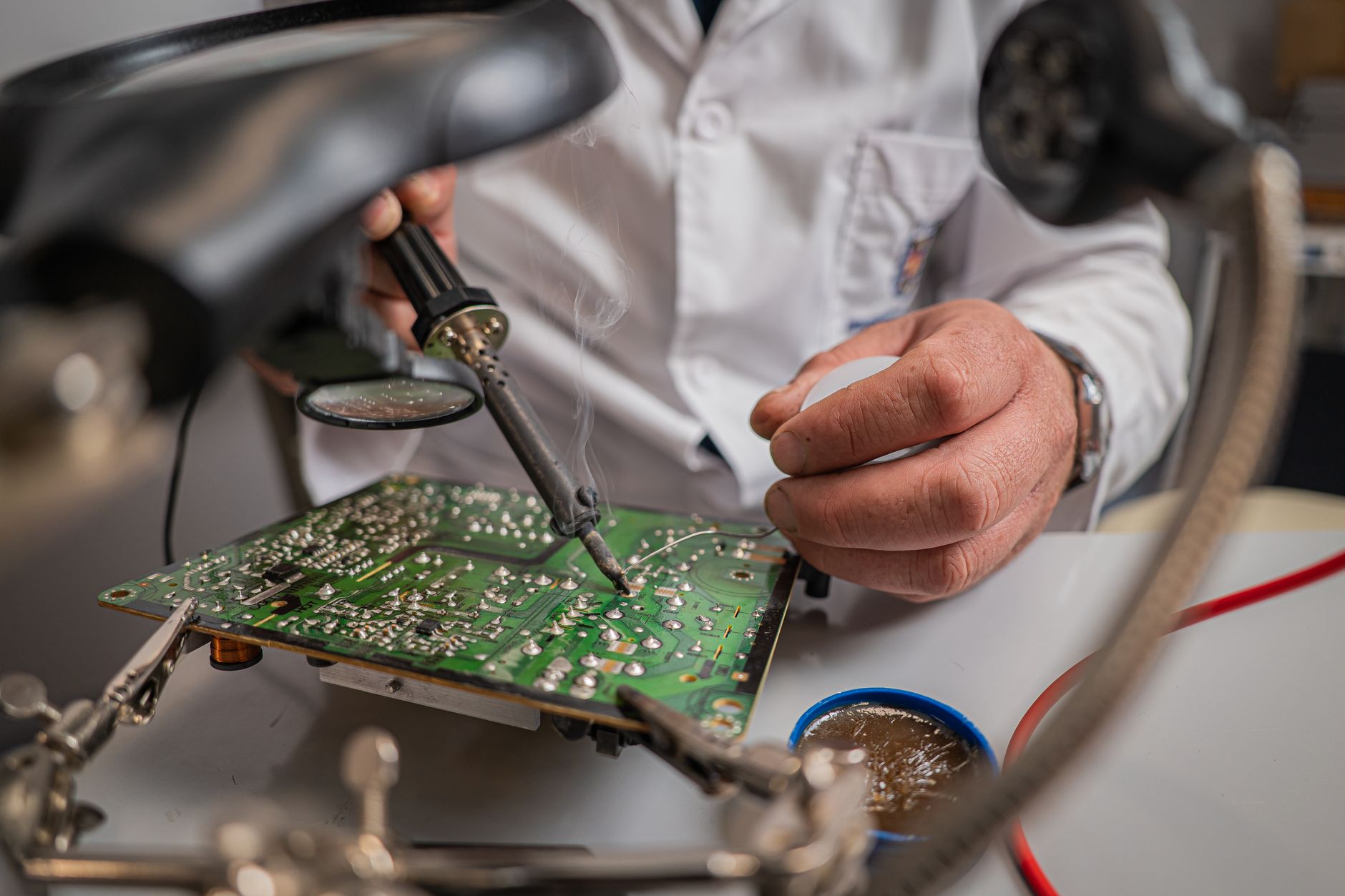
Types of PCBA Assembly Methods Used in Manufacturing
Three assembly methods define modern PCBA manufacturing: Surface Mount Technology (SMT), Through-Hole Technology (THT), and mixed technology, each suited to specific product demands.
SMT vs THT vs Mixed Technology: Key Differences
Surface Mount Technology (SMT) places components directly onto pads on the board surface, where solder paste bonds them during reflow. This approach supports high component density and automated high-speed placement, making it the standard method for compact consumer electronics, smartphones, and high-volume production runs.
Through-Hole Technology (THT) feeds component leads through drilled holes in the board and solders them on the opposite side. The mechanical bond created is significantly stronger than a surface pad joint, which is why connectors, transformers, and components exposed to vibration or thermal cycling rely on THT.
Mixed technology combines both methods on a single board. Because SMT components are reflowed first, a second soldering pass is required for THT components. Selective soldering machines apply solder only to targeted THT joints, leaving the already-reflowed SMT areas undisturbed and preventing thermal damage to sensitive components.
How Product Type Drives Assembly Method Selection
The PCBA assembly process method follows directly from what the board must do. High-frequency RF boards favor SMT because shorter signal paths reduce parasitic inductance and signal loss. Industrial power boards use THT for its thermal and mechanical durability under load.
Medical and aerospace boards frequently combine both, mixed technology with tighter process controls, additional inspection steps, and full traceability to meet standards such as IPC-A-610 Class 3.
How Quality Is Assured and Tested in PCBA Assembly
No single test catches every defect in the PCBA assembly process, manufacturers layer multiple inspection methods to close the gaps each one leaves.
Testing follows a fixed sequence. Manual visual inspection runs first and catches gross defects like missing components or obvious solder bridges, but it misses fine-pitch joints and internal voids. Automated Optical Inspection (AOI) uses cameras and pattern-matching algorithms to scan solder joints and component placement at high speed; it excels at surface defects but cannot see beneath components. X-ray inspection fills that gap, it reveals hidden solder joints under BGAs and QFNs, including voids and bridging invisible to optical systems. In-Circuit Testing (ICT) uses a bed-of-nails fixture to probe individual nodes and verify component values, shorts, and opens, but requires a custom fixture for each board design. Functional Circuit Testing (FCT) powers the board and tests it against its intended behavior; it validates the assembly as a system but cannot always pinpoint which component caused a failure. Flying Probe Testing replaces the ICT fixture with movable probes, slower per board, but cost-effective for low-volume or prototype runs where building a dedicated fixture is impractical.
IPC-A-610 is the globally recognized acceptability standard for electronic assemblies. It defines three workmanship classes: Class 1 covers general-purpose electronics with minimal performance requirements, Class 2 applies to dedicated-service products where extended life is expected, and Class 3 governs high-reliability applications, military, aerospace, and medical, where failure is not acceptable. The class selected directly sets inspection criteria and reject thresholds; a solder joint acceptable under Class 1 may be a defect under Class 3.
ISO 9001 operates at the process level, not the product level. It governs how a manufacturer documents procedures, monitors output, and drives continuous improvement. Buyers use ISO 9001 certification as a baseline qualification signal, it confirms a supplier has a controlled system, not that every board is perfect.
Common PCBA Defects, Failure Modes, and How to Troubleshoot Them
Four defects account for the majority of PCBA rework. Solder bridges, two adjacent pads shorted by excess solder, trace back to over-deposited paste or a misaligned stencil; the fix is aperture adjustment and stencil realignment. Tombstoning occurs when one end of a passive component lifts during reflow because uneven heating creates an imbalanced surface tension pull; correcting the thermal profile or pad geometry resolves it. Cold joints appear dull and granular because insufficient heat or board movement during cooling prevented proper solder flow; the root cause is usually a reflow oven profile that ramps too slowly or a conveyor speed set too high. Missing components result from pick-and-place feeder jams or empty tape reels; AOI catches these immediately after placement, and feeder maintenance schedules prevent recurrence.
Key Considerations for Choosing a PCBA Manufacturer and Managing Costs
The right PCBA manufacturer balances certification depth, regional trade-offs, and DFM capability, not just the lowest quoted price per board.
How Assembly Costs Compare Across Manufacturing Regions
Several levers drive cost through the PCBA assembly process before a single component is placed. Board layer count raises material and lamination expense directly. Assembly method matters too, SMT is generally more cost-efficient at volume, while through-hole and mixed-technology builds require more manual labor and fixture investment. Component sourcing complexity (long lead times, single-source parts, or obsolete ICs) adds procurement overhead that lands on the buyer’s invoice.
Order volume and turnaround time are the two levers buyers control most directly. Low-volume, fast-turn builds carry a premium; high-volume programs with flexible lead times push unit costs toward budget-friendly territory.
Regionally, high-volume and cost-sensitive production gravitates toward Asia, particularly China, Vietnam, and Malaysia, because of labor cost advantages and the density of component supply chains within short logistics distances. North American and European manufacturers compete on different strengths: tighter IP protection, regulatory compliance for defense and medical programs, faster design iteration cycles, and easier communication for high-mix or low-volume programs where engineering collaboration matters more than unit economics.
Quality Certifications Required for Different Industries
Certifications signal specific process control capabilities, not just audit paperwork. For aerospace, require IPC-A-610 Class 3, the workmanship standard for high-reliability electronics, alongside AS9100, which adds traceability and configuration management controls the sector demands. Medical device assemblies call for ISO 13485, which governs the quality management system around design, production, and post-market surveillance. Automotive programs increasingly require IATF 16949, which layers process failure-mode controls on top of ISO 9001. Any product entering North American consumer or industrial markets should carry UL certification to satisfy safety compliance at the point of sale.
Beyond certifications, evaluate suppliers on DFM support depth, component sourcing transparency, testing coverage (ICT, functional, AOI, X-ray), and how structured their New Product Introduction process is. Weak DFM support shifts rework costs directly to the buyer, a supplier who flags a pad geometry issue before stencil printing costs far less than one who ships a defective first article.

Frequently Asked Questions
What is the difference between PCB fabrication and PCBA assembly?
PCB fabrication produces the bare board, the laminated substrate with etched copper traces, drilled holes, and applied solder mask. PCBA assembly is the subsequent stage where components (resistors, ICs, connectors) are placed and soldered onto that bare board to create a functional circuit. Think of fabrication as building the chassis and assembly as installing the engine.
How long does the PCBA assembly process typically take from design to finished board?
Lead times range from 1 day for expedited prototype runs to several weeks for high-volume production orders, depending on board complexity, component availability, and the testing requirements specified. Sourcing long-lead components is usually the biggest schedule driver, locking down your bill of materials early compresses the overall timeline more than any other single action.
What files does a manufacturer need to start PCBA assembly?
At minimum, a manufacturer needs Gerber files for the bare board, a bill of materials (BOM) listing every component with part numbers and quantities, and a pick-and-place (centroid) file that maps each component’s X/Y coordinates and rotation on the board. Some manufacturers also request assembly drawings and IPC netlist files for electrical testing setup.
Can PCBA assembly handle both prototype quantities and high-volume production?
Yes, most contract manufacturers support both, though the processes differ. Prototype runs often use flexible stencil setups and manual inspection to validate the design quickly, while high-volume production uses dedicated tooling, automated optical inspection (AOI), and in-circuit testing (ICT) to maintain yield at scale. Confirming your manufacturer’s minimum order quantities and setup fees before committing avoids costly surprises at either volume level.
Conclusion
The PCBA assembly process rewards preparation. Boards that arrive at a manufacturer with clean Gerber files, a verified BOM, and a clear test specification move through solder paste printing, component placement, reflow, and inspection without costly rework loops. Choosing the right assembly method, SMT, THT, or mixed, before layout begins saves more time than any downstream fix.
As a concrete next step, run a DFM (Design for Manufacturability) check on your current board files before submitting them. Most contract manufacturers offer this as a free pre-production review, request one, review the flagged items, and resolve them before a single stencil is cut.
Recommended Articles
Explore more from our content library:
