

PCBA design for manufacturability (DFM) is the practice of designing printed circuit board assemblies so they can be produced reliably, efficiently, and at the lowest viable cost. Applied early in the design cycle, DFM reduces defect rates, shortens lead times, and prevents expensive respins. Key decisions, trace width, component spacing, pad geometry, and panelization, directly determine whether a board moves smoothly from prototype to high-volume production or stalls in costly rework loops.

What Is PCBA Design for Manufacturability and Why Does It Matter?
PCBA design for manufacturability is a set of engineering rules applied during layout to ensure a board can be fabricated and assembled within real process constraints.
DFM is often conflated with DFA (design for assembly), but the two address different problems. DFM governs fabrication constraints, trace widths, drill sizes, copper clearances, and plane geometry. DFA governs how components are placed and joined during assembly, covering things like pick-and-place access, solder paste deposit volume, and reflow thermal profiles. Both apply to a PCBA project, but they operate at different stages of the manufacturing process.
The cost argument for early DFM review is well-established. A layout-stage fix costs roughly 10 times less than the same correction caught during first-article inspection or production. That gap widens further when a respin requires new tooling or delays a product launch.
A concrete example of a DFM rule with real electromagnetic consequences is the 20H rule: the power plane edge should be set back from the board edge by a distance equal to 20 times the dielectric thickness between the power and ground planes. That setback reduces fringe flux and limits EMI radiation before a single board is fabricated, no lab measurement required.
“Applying DFM principles at the schematic stage rather than after layout is complete can reduce total project cost by 30 percent or more — the earlier you engage your contract manufacturer, the fewer surprises you encounter at the fab floor.” — Lee Ritchey, Founder and Principal at Speeding Edge
How DFM Differs Between Prototype and High-Volume Production Runs
Prototype DFM priorities center on flexibility and speed. A contract manufacturer running five boards will tolerate tighter component spacing or manual rework steps that would be unacceptable at scale.
High-volume production shifts the priorities to yield, repeatability, and panelization efficiency. Panel utilization directly affects per-unit cost, a poorly arranged panel can waste 20–30% of raw laminate. Solder joint consistency and automated optical inspection (AOI) pass rates become the controlling metrics.
DFM is not a checklist an engineer runs at tape-out. It works best as a shared responsibility between the design team and the contract manufacturer, with the CM’s process capabilities, minimum annular ring, supported hole aspect ratios, paste aperture rules, feeding back into the layout before the first Gerber file is generated. According to Sierra Circuits’ DFM issues guide, engaging your CM’s process capabilities document before routing begins is one of the highest-leverage steps a design team can take.
How to Design a PCB With Manufacturability in Mind
Manufacturable PCB layouts follow explicit dimensional rules and machine-process constraints that prevent defects before a single board enters production.
Assembly-Specific Constraints for Pick-and-Place and Reflow
Fiducial marks are the first thing pick-and-place machines use to orient a panel. Place a minimum of three fiducials per panel, at least 5 mm from the board edge, omitting them forces the machine to estimate registration, which shifts component placement and drives up defect rates on fine-pitch parts.
Component pitch below 0.4 mm requires vision-system calibration and slows machine throughput measurably. On 0402 passives and smaller, asymmetric pad sizes create uneven surface tension during reflow, one pad wets before the other, lifting the component vertically in a defect known as tombstoning.
Solder alloy consistency matters just as much as pad geometry. Running mixed Sn63/Pb37 (eutectic, peak ~183 °C) and SAC305 (lead-free, peak ~250 °C) on the same board creates a reflow profile conflict: the temperature needed to fully melt SAC305 can damage components rated for the lower eutectic profile. Specify one alloy system per board and confirm it with your CM before layout is finalized.
Trace Width, Spacing, and Component Placement Rules That Protect Yield
PCBA design for manufacturability starts with IPC-2221, which sets 0.1 mm (4 mil) as the minimum spacing for external conductors at low voltage. Etching is a subtractive chemical process, traces closer than 0.1 mm leave insufficient copper separation, and etchant undercut bridges the gap, creating shorts that visual inspection often misses.
Thermal relief connections on through-hole pads are equally non-negotiable. A pad connected directly to a solid copper pour acts as a heat sink during wave soldering, the pour draws heat away faster than the solder joint can form, producing a cold joint with poor mechanical and electrical integrity. Spoke-style thermal reliefs (typically four spokes at 45° or 90°) restrict heat flow to the pad and allow consistent joint formation.
Keep component placement directional: orient all polarized parts the same way and align passive arrays in a single axis. This reduces the number of board rotations during inspection and rework, cutting handling time per board.
“Consistent component orientation is one of the simplest DFM improvements a layout engineer can make — it costs nothing in routing time but measurably reduces assembly errors and inspection time at the factory.” — Mark Finstad, Senior Application Engineer at Flexible Circuit Technologies
The Most Common DFM Issues and How to Avoid Them
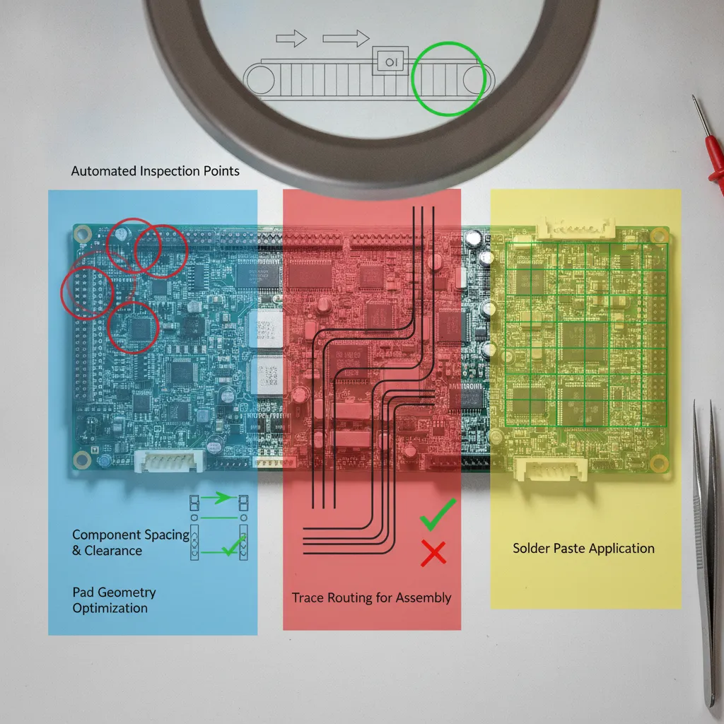
Five defect types—annular ring failures, acid traps, silkscreen over pads, missing solder mask expansion, and courtyard violations—cause the majority of PCBA design for manufacturability rejections. According to Sierra Circuits, these five categories account for a disproportionate share of first-article failures across all board complexity levels.
Each has a clear root cause and a one-line fix:
- Insufficient annular ring: Drill wander breaks the copper ring, creating open vias. Fix: maintain a minimum 0.3 mm annular ring on all vias.
- Acid traps (acute-angle traces): Traces meeting below 90° trap etchant and cause over-etching at the junction. Fix: route all trace junctions at 90° or 45°; enable the acute-angle DRC rule in your layout tool.
- Silkscreen over pads: Ink on a soldering pad contaminates the joint. Fix: set a silkscreen-to-pad clearance of at least 0.1 mm in your design rules.
- Missing solder mask expansion: IPC-7351 recommends 0.05–0.1 mm expansion per side. Too little causes solder bridging; too much exposes adjacent copper and risks shorts.
- Incorrect courtyard clearances: Overlapping component courtyard boundaries make pick-and-place impossible. Fix: enforce a minimum 0.25 mm courtyard-to-courtyard gap across all footprints.
Before and After: Annular Ring on a 6-Layer Board
A 6-layer board designed with 0.2 mm annular rings on 0.3 mm vias recorded a 12% open-via defect rate in production. Increasing the annular ring to 0.3 mm dropped that defect rate to under 1%—a change that costs nothing in design time but eliminates a significant rework burden at the factory.
The fix required editing a single design rule in the constraint manager and re-running DRC. No layout changes were needed beyond the two vias that fell outside the new rule.
Design Rule Checks That Catch DFM Problems Early
Run these five DRC checks before exporting Gerber files—catching violations here is orders of magnitude cheaper than catching them after fabrication.
- Clearance check: Confirms copper-to-copper spacing meets fab minimums.
- Short-circuit check: Flags nets that share copper unintentionally.
- Unconnected net check: Catches missing connections before the board is etched.
- Hole-to-copper check: Verifies drill hits won’t damage adjacent traces or planes.
- Silkscreen-to-pad overlap check: Removes ink from soldering surfaces automatically.
Both Altium Designer and KiCad include acid-trap detection, but the rule is disabled by default in many project templates. Enable it manually before your first DRC run on any new design.
How DFM Decisions Affect Cost, Timeline, and Project ROI
DFM decisions made during layout directly determine unit cost, NRE exposure, and whether a product ships on schedule or burns weeks in rework.
Trade-Offs Between Design Complexity and Manufacturing Cost
Layer count is the single largest cost lever on a bare board. Moving from a 4-layer to a 6-layer stackup typically increases PCB unit cost by 40–60% at low volumes, a trade-off that belongs in the PCBA design for manufacturability review, not just the schematic phase.
Via technology carries a similar penalty. Via-in-pad and blind/buried vias add 20–35% to fabrication cost compared to standard through-hole vias. Engineers should justify each one against genuine routing necessity; using them for layout convenience quietly inflates the BOM before a single component ships.
Panelization efficiency is where small decisions have outsized impact. A board that panels 4-up instead of 2-up at the same panel size halves the per-unit fab cost, no design change required, just deliberate board outline and spacing choices made early.
The cost of a respin makes the timeline argument concrete. NRE costs for a single respin average $5,000–$25,000 depending on board complexity and fab tier. One DFM-driven respin can erase the ROI of an entire product revision cycle.
The timing of discovery matters as much as the defect itself. A DFM failure caught during layout review adds hours to a schedule. The same failure caught at incoming inspection adds 2–4 weeks minimum, plus the carrying cost of idle assembly capacity and delayed customer commitments.
DFM Tools and Collaboration Workflows for Design Engineers and Manufacturers
The right EDA tool and a structured communication workflow cut PCBA design for manufacturability errors before they reach the fab floor, saving respins and weeks of delay.
How Cadence, Altium, and Mentor DFM Tools Compare
Each major EDA platform handles DFM analysis differently, and the gap matters most when you work with high-volume contract manufacturers.
- Cadence Allegro X builds DFM analysis directly into the layout environment, flagging constraint violations in real time as you route. According to Cadence’s DFM analysis overview, engineers see clearance, annular ring, and solder mask issues without exporting a separate file, which significantly reduces iteration time on complex multilayer designs.
- Altium Designer relies on its built-in Design Rule Check (DRC) for basic validation, then depends on third-party tools, most commonly Valor NPI, for CM-grade DFM output. The workflow adds a step but remains widely used.
- Mentor Xpedition integrates Valor NPI natively, which makes it the strongest option for high-volume CM collaboration. Engineers export files the CM can review without format conversion or manual interpretation.
Valor NPI, now part of Siemens EDA, is the de facto standard for CM-side DFM review. Engineers who export Valor-compatible outputs reduce back-and-forth with fabricators by an estimated 30–40%, because the CM receives structured, machine-readable data rather than annotated PDFs.
“The single biggest efficiency gain in PCB manufacturing comes when design teams and contract manufacturers share a common DFM language from day one — structured data formats like Valor NPI eliminate the interpretation errors that cause most preventable respins.” — Happy Holden, PCB Industry Technologist and Contributing Editor at I-Connect007
Communication Workflows Between Engineers and Contract Manufacturers
Most DFM problems trace back to a single process failure: the CM receives Gerber files before they know the board’s requirements. Share stackup requirements, controlled-impedance targets, and panelization specs with your CM before layout begins, not after submission.
Your fab drawing package should include four items that prevent interpretation errors:
- A complete drill legend with finished hole sizes and tolerances
- Impedance callouts referencing specific layers and trace widths
- Surface finish specification, HASL, ENIG, or OSP, with any exemptions noted
- IPC class designation (Class 2 or Class 3) so the fabricator applies the correct acceptance criteria
Set a formal DFM review gate at 80% layout completion. That point is late enough that copper pours, via structures, and component placement are stable, but early enough that the team can act on CM feedback without a full respin.
Frequently Asked Questions
What is the 20H rule in PCB design and how does it relate to DFM?
The 20H rule states that the power plane should be recessed inward from the ground plane edge by a distance equal to 20 times the dielectric thickness between the two planes. This reduces electromagnetic flux fringing at board edges, which lowers radiated emissions. From a DFM standpoint, applying the 20H rule during layout prevents costly EMC failures that would otherwise require a board spin, one of the most expensive post-fabrication corrections a design team can face.
How do DFM choices affect PCB unit pricing and NRE costs?
DFM choices directly set your unit price and non-recurring engineering costs, a board with 4-mil trace/space rules costs significantly more per panel than one designed to a 6-mil standard. Tight via-to-copper clearances, blind or buried vias, and non-standard board thicknesses each add fabrication steps that raise NRE charges. Designing to a contract manufacturer’s stated process capabilities from the start typically cuts unit cost by 15–30% compared to designs that require process exceptions.
What surface finish should I specify for best manufacturability, HASL, ENIG, or OSP?
HASL suits through-hole-heavy boards on a tight budget; ENIG is the better choice for fine-pitch SMD components and boards requiring a flat, oxidation-resistant surface; OSP works well for single-reflow assemblies where cost is the priority. ENIG’s flat pad surface makes it the most forgiving finish for 0402 passives and QFN packages, where coplanarity directly affects solder joint yield. Confirm your CM’s preferred finish early, switching after Gerber submission can delay fabrication by several days.
When in the design process should I run a DFM review?
Run your first DFM review at schematic completion, before layout begins, catching component availability and footprint issues at this stage costs nothing to fix. Run a second automated DFM check immediately after placing components and routing critical nets, then a final review before releasing Gerbers. Waiting until tape-out to run DFM is the single most common cause of costly design respins.
What information should I include in my fab drawing package to avoid DFM rejections?
A complete fab drawing package should include a drill legend with finished hole sizes and tolerances, impedance callouts tied to specific layers and trace widths, a surface finish specification with any exemptions noted, and an explicit IPC class designation (Class 2 or Class 3). Missing or ambiguous information in any of these four areas is a leading cause of fabrication holds and delays. Providing this data upfront reduces back-and-forth with your CM and prevents misinterpretation that can add days to your lead time.
Conclusion
PCBA design for manufacturability is not a final checklist, it is a set of decisions made at schematic, layout, and documentation stages that determine yield, cost, and delivery time before a single board is fabricated. Three actions move the needle most: confirm component footprints against your CM’s land pattern library before routing, run automated DFM checks at component placement rather than tape-out, and specify surface finish and via type only after reviewing your CM’s process capabilities document.
As a concrete next step, request your contract manufacturer’s DFM design rules document and compare it against your current schematic’s component list, mismatches found at that stage cost nothing to resolve.
Recommended Articles
Explore more from our content library:
